Detector Development Lab (DDL)
Pioneering Advanced Detectors
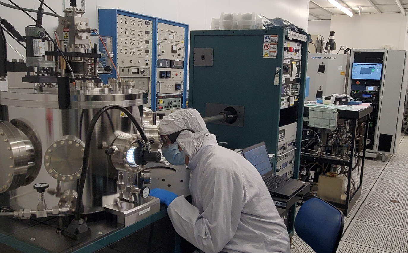
The DDL is a microelectronics fabrication facility dedicated to the development of advanced detectors, micro-electrical-mechanical-systems (MEMS), nano-scale devices, circuits, and components for NASA’s missions. The laboratory is built around a 4,800 square foot, ISO 5 cleanroom, housing an extensive array of semiconductor processing equipment to perform full-scale, custom, wafer fabrication up to 200mm. The lab contains a large variety of semiconductor fabrication equipment for optical and electron beam lithography, wet and dry etching, oxidation, diffusion, thin film deposition, metallization and device characterization.
